Understanding the Differences Between PCB Assembly and Fabrication
Printed circuit boards (PCBs) are the foundation of modern electronics. The process of circuit board assembly involves adding electronic components to the fabricated board, which includes its layers and holes. This transformation of raw materials into a functional platform for connections is crucial. While PCB fabrication creates the board itself, circuit board assembly is the step that integrates the necessary parts to enable the board to perform specific functions.
The primary distinction lies in their roles: fabrication focuses on constructing the board, whereas assembly is about enhancing it with components to ensure it operates effectively. Over 70% of PCBs are utilized in electronics, computers, and telecommunications, underscoring the significance of both processes. From cars projected to reach $13.39 billion by 2030 to smart home devices, PCBs play a vital role in advancing technology.
Key Takeaways
PCB fabrication builds the board, while assembly adds parts to use it.
Knowing the difference between fabrication and assembly helps make better PCBs.
Main steps in fabrication include making designs, cutting, and drilling holes.
In assembly, adding solder paste and placing parts correctly is important.
Checking often during both steps ensures the product works well and lasts.
Using tools like AOI and X-ray finds and fixes problems early in assembly.
Picking good materials for fabrication affects how well it works and costs.
Both fabrication and assembly must work together to make reliable electronics.
PCB Fabrication: Making the Printed Circuit Board
Purpose of PCB Fabrication
PCB fabrication is how we make printed circuit boards. It turns a design idea into a real board for electronics. This process ensures the board works well, lasts long, and is reliable. Many industries, like healthcare and electronics, need good PCBs for their devices. For example, medical machines and cameras need precise boards to work properly. By focusing on being accurate and fast, fabrication helps create strong boards for many uses.
Key Steps in PCB Fabrication
Designing the PCB Layout
The first step is designing the PCB layout. Special software is used to draw a plan showing how parts connect. This plan makes sure the board will work as needed. It includes where parts go, how traces connect, and how layers are arranged.
Creating the PCB Layers
After the design is ready, the layers are made. Modern PCBs often have many layers for complex circuits. Each layer is a thin sheet of copper on a non-conductive base. These layers are stacked to save space and fit more circuits.
Etching and Laminating the Board
Etching removes extra copper, leaving only the needed circuits. A mask protects the copper while chemicals remove the rest. After etching, layers are pressed together with heat to make one board.
Drilling and Plating Holes
Holes are drilled for parts and to connect layers. These holes are coated with copper to ensure proper connections. This step is very important for double-sided and multilayer boards.
Applying Solder Mask and Silkscreen
A solder mask is added to protect copper and stop solder mistakes. This thin layer also makes the board stronger. The silkscreen adds labels and symbols to help during assembly and show important details.
Adding solder masks made soldering easier and reduced mistakes like bridges between pins. This became a standard in the industry.
Final Inspection and Testing
Before assembly, the board is checked and tested. Electrical tests make sure circuits work correctly. Visual checks and other inspections find and fix any problems.
Step Number | Step Description | Main Activities |
|---|---|---|
1 | Preparation | Checking design, setting production rules, choosing methods |
2 | Inner Layer | Cleaning, adding dry film, exposing images |
3 | Outer Layer | Removing burrs, etching, plating |
4 | Plating | Adding copper and tin patterns |
5 | Solder Mask | Preparing surfaces, coating, exposing images |
6 | Surface Finish | Adding finishes like HASL, silver, or ENIG |
7 | Profile | Cutting or shaping the board |
8 | ET Testing | Checking circuit connections and isolation |
9 | QC Inspection | Doing visual and mechanical checks |
Materials Used in PCB Fabrication
The materials used in PCB fabrication affect how the board works and costs. FR-4, a strong epoxy material, is the most common base because it handles heat and electricity well. Some boards, like those for medical devices, use special materials like polyimide or ceramic for better performance. Copper is used for circuits, while solder masks and silkscreens protect and label the board.
Thermal reliability means the board can handle high heat.
Mechanical reliability keeps the board safe from damage.
Electrical stability ensures the board works under different conditions.
Chemical reliability protects the board from things like water and rust.
The cost of materials depends on layers, design, and use. For example, medical PCBs often use high-quality materials for safety and performance.
Challenges in PCB Fabrication
Making PCBs comes with problems that affect quality and reliability. Knowing these problems helps fix issues and improve production.
Heat Management Problems
Getting rid of heat is very important in making PCBs. If heat isn't handled well, parts can overheat and stop working. Poor heat relief can make soldering harder. Blocked airflow makes it tough to cool the board. These problems happen often in crowded boards with little space for cooling.
Physical Limitations
Stress can damage the shape and strength of PCBs. Bending, tiny cracks, or warping can mess up layers. Thin or very large boards bend more easily, causing parts to misalign. In cars and planes, constant shaking can break solder joints or crack circuits.
Heat-Related Damage
High heat for a long time can harm PCB parts. Too much heat can cause systems to fail completely. Heating and cooling over and over weakens solder joints, breaking connections. These problems are big for industries needing strong boards, like medical tools and telecom.
Tip: To avoid these problems, design carefully, use good materials, and test thoroughly during PCB fabrication.
PCB Assembly: Completing the Circuit Board Assembly
Purpose of PCB Assembly
PCB assembly turns a plain board into a working one. This is done by adding electronic parts to it. The process makes sure the board works in devices like phones and medical tools. Without PCB assembly, modern electronics wouldn’t work properly. It also affects how long and how well the product will last.
PCB assembly is very important in today’s manufacturing world.
The global PCB market may grow from $80.33 billion in 2024 to $96.57 billion by 2029, growing 4.87% each year.
Over 1.3 billion smartphones are shipped every year, all needing PCBs.
Smart home devices depend on good PCBs to work well and stay affordable.
Some manufacturers also help by improving designs and managing supplies. These extra services make PCB assembly a key part of making products.
Key Steps in PCB Assembly
Solder Paste Application
The first step is applying solder paste. A stencil is placed on the board, and paste is spread over it. The paste has tiny metal bits and flux to help parts stick during soldering. It’s important to apply the paste carefully to avoid mistakes.
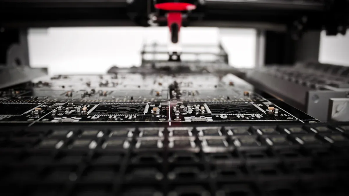
Component Placement
Next, parts are placed on the board. Machines called pick-and-place machines do this job. They put parts like chips and resistors onto the solder paste. Correct placement is needed for the board to work right.
Soldering (SMT and Through-Hole)
Soldering attaches the parts to the board. SMT soldering uses heat to melt the paste and stick parts. Through-hole soldering involves putting part leads into holes and soldering them by hand or machine. Both methods are needed to make the board work.
Inspection and Quality Control
After soldering, the board is checked for problems. Automated Optical Inspection (AOI) looks for misplaced parts or bad soldering. Statistical Process Control (SPC) studies data to find and fix issues. These checks make sure the board is high quality.
Step | Analysis Process | Performance Metrics |
|---|---|---|
5 | Automated Optical Inspection (AOI) | Checks solder quality, size, and if it meets standards. |
6 | Statistical Process Control (SPC) | Studies data to find and fix defects. |
Functional Testing
The last step is testing the board to see if it works. This step copies real-life conditions to check if the board performs well. Testing ensures the board meets industry rules and works as it should.
Tools and Equipment Used in PCB Assembly
PCB assembly uses special tools to work quickly and accurately. Machines like pick-and-place, reflow ovens, and wave soldering are common. Inspection tools like AOI and X-ray machines find problems and ensure quality. For car PCBs, tough tests check if they can handle heat and shaking.
Inspection Method | Description | Key Parameters |
|---|---|---|
Manual Inspection | Looking at the board to find problems. | Checks for bending, size, solder issues, and damaged parts. |
X-ray Inspection | Uses machines to find hidden problems in solder and parts. | Finds solder issues, damaged parts, and gaps in solder joints. |
Rules like IPC-A-610 and IPC-6012 guide the process. These rules help make strong and reliable boards for many uses.
Challenges in PCB Assembly
PCB assembly (PCBA) has many challenges that affect quality and reliability. Knowing these problems early helps fix them and ensures a smooth assembly process.
1. Wrong Component Placement
Placing parts incorrectly is a common issue in PCBA. Machines are precise, but mistakes happen due to bad programming, damaged parts, or misaligned stencils. Misplaced parts can cause short circuits or failures, especially on crowded boards.
2. Soldering Problems
Soldering is very important but can cause issues. Problems like solder bridges, weak joints, or not enough solder can hurt the board's performance. For example, an aerospace company had flight system failures due to bad soldering. This shows why careful checks during soldering are crucial.
Tip: Use tools like AOI and X-ray machines to find soldering problems early and avoid expensive fixes.
3. Temperature Issues
Temperature control is key for soldering and keeping parts safe. If the reflow oven's heat is not set right, soldering may fail, or parts might get damaged. Keeping the right temperature ensures solder melts properly and parts stay unharmed.
4. Damaged Components During Assembly
Delicate parts need careful handling during assembly. Too much force, static electricity, or bad storage can ruin parts. Cross-section analysis can check solder joints and find flaws that might cause failures.
5. Design Problems for Manufacturing
Design for Manufacturing (DFM) makes sure the PCB design is easy to assemble. Mistakes like parts being too close or bad solder pad designs can make assembly harder. These errors increase defects and raise costs.
Cross-section analysis checks layer alignment, plating, and solder joints for quality.
It finds flaws that could cause failures, which is vital for reliable devices.
6. Quality Control Challenges
Keeping quality consistent in PCBA needs strong checks. Common problems include:
Wrong component placement
Soldering problems
Temperature issues
Damaged components
Design mistakes
Each issue can lower the board's performance and reliability. Fixing these problems early improves the overall assembly process.
Note: Regular testing and inspections with advanced tools like AOI and X-ray machines can reduce defects and improve production success.
PCB Fabrication vs. PCB Assembly: Key Differences
Differences in Purpose
PCB fabrication and assembly have different jobs in making circuit boards. Fabrication builds the board's structure. This includes making layers, cutting copper paths, and getting the board ready for use. The main goal is to create a strong and affordable base for circuits. For example, prototype boards can be made in 1-2 days, helping designers test ideas quickly.
PCB assembly, however, turns the board into a working circuit by adding parts. This step focuses on making sure the board works well in devices like phones or medical tools. Assembly is harder and costs more because parts must be placed and soldered carefully. While fabrication aims for speed, assembly ensures the board is reliable and performs well.
Differences in Processes
The steps in fabrication and assembly are very different. Fabrication starts with designing the board, then making and shaping the layers. Drilling holes, adding copper, and applying solder masks prepare the board for assembly. These steps change raw materials, like copper sheets, into detailed circuit designs.
Assembly, on the other hand, involves adding solder paste, placing parts, and attaching them to the board. Machines like pick-and-place tools and reflow ovens make this process fast and accurate. Inspections, such as AOI and X-ray checks, ensure quality. For example, AOI finds misplaced parts, while X-rays spot hidden solder problems. The final step tests the board to make sure it works in real-life situations.
Purpose | |
|---|---|
Solder Paste Inspection | Checks if solder paste is applied correctly. |
X-ray Inspection | Finds hidden problems, like gaps in solder joints. |
Automatic Optical Inspection (AOI) | Spots visible issues, like crooked parts or bad soldering. |
Functional Testing | Makes sure the board works before being shipped. |
Differences in Materials and Tools
The materials and tools for fabrication and assembly are unique to their tasks. Fabrication uses items like copper sheets, prepreg, and chemicals for etching. These materials affect how the board handles heat, pressure, and electricity. For instance, FR-4 is a popular material because it is strong and heat-resistant. Costs depend on the material's thickness and quality.
Assembly needs electronic parts like resistors, chips, and capacitors. Tools such as pick-and-place machines, reflow ovens, and wave soldering equipment are used to attach these parts. Inspection tools, like AOI and in-circuit testers, check that the board meets quality standards. The table below shows some important materials and tools for both processes:
Category | Description | Cost Impact |
|---|---|---|
Copper-Clad Laminates | Base material with copper attached to a sturdy layer. | High, as it affects the board's strength and performance. |
Pick-and-Place Machines | Places parts on the board automatically during assembly. | High, because they need to be fast and precise. |
Solder Mask | A layer that protects copper and prevents solder mistakes. | Moderate, but important for making the board last longer. |
Reflow Ovens | Heats solder paste to attach parts securely to the board. | High, as they are key to creating strong and reliable connections. |
By learning these differences, you can see how fabrication and assembly work together to make useful circuit boards.
Differences in Outcomes
PCB fabrication and assembly create different results for different jobs. Fabrication makes the board's structure, including layers, copper lines, and holes. This step gets the board ready for the next process. The result is a plain board that supports electronic circuits. Without this step, adding parts would not be possible.
PCB assembly, or PCBA, turns the plain board into a working circuit. It adds parts like resistors, capacitors, and chips to make the board work. The result is a fully working PCB used in devices like phones, medical tools, and cars. For example, a PCBA in a phone allows features like touchscreens and Wi-Fi.
The quality of these results depends on being precise and accurate. Fabrication focuses on making a strong base, while assembly ensures the board works well. Together, these steps create a product that meets standards and works as expected.
How Fabrication and Assembly Work Together
Fabrication and assembly depend on each other to make working PCBs. Fabrication builds the board's base, and assembly adds the parts that make it work. A poorly made board can cause problems like misaligned layers or bad soldering spots during assembly.
The table below shows how these steps work together:
Process Step | Description | Technology Used | Purpose |
|---|---|---|---|
Bare Board Fabrication | Making the PCB with copper lines. | Etching, Drilling | Create a base for adding parts. |
Solder Paste Application | Spreading solder paste on pads. | Stencil Printing | Get pads ready for attaching parts. |
Component Placement | Adding parts like chips and resistors. | Pick-and-Place Machines | Place parts quickly and correctly. |
Reflow Soldering | Attaching parts to the board. | Reflow Ovens | Make strong connections between parts and board. |
Inspection | Checking solder and part placement. | AOI and X-ray | Find mistakes in soldering or placement. |
Functional Testing | Testing the finished board. | Automated Test Equipment | Ensure the board works as designed. |
Each step in fabrication and assembly helps make the final product. For example, etching and drilling during fabrication create the right layout for parts. Reflow soldering during assembly makes strong connections between parts and the board. Both processes must work together to make a reliable PCBA.
By learning how fabrication and assembly connect, you can understand the effort behind making modern electronics. This knowledge helps in designing or producing PCBs better.
Knowing how PCB fabrication and assembly (PCBA) differ is important. Fabrication builds the board's base, while PCBA adds parts to make it work. Both steps are needed to create dependable electronics. Fields like cars and healthcare need top-quality PCBA for safety and performance. The rise of smart gadgets and electric cars shows why better PCB making matters. Learning these steps helps you create modern, efficient products for today’s technology.
FAQ
1. What is the main difference between PCB fabrication and PCB assembly?
PCB fabrication makes the board's structure, like layers and copper paths. PCB assembly adds parts to make the board work. Fabrication builds the base, while assembly finishes the circuit.
2. Can one company handle both PCB fabrication and assembly?
Yes, some companies do both jobs. This makes things easier by reducing communication problems and ensuring the board and parts fit well together.
3. How long does PCB fabrication and assembly take?
Fabrication usually takes 1–2 weeks, depending on size and design. Assembly takes a few days to a week. Prototypes are faster, often done in 1–3 days.
4. What materials are commonly used in PCB fabrication?
FR-4 is popular because it’s strong and handles heat well. Other materials include polyimide for flexibility and ceramic for high performance. Copper is used for circuits, and solder masks protect the board.
5. What tools are essential for PCB assembly?
Important tools include pick-and-place machines for adding parts, reflow ovens for soldering, and inspection tools like AOI and X-ray machines. These tools ensure accuracy and quality.
6. Why is inspection important in PCB assembly?
Inspection checks if the board works and meets standards. Tools like AOI and X-ray find problems like misplaced parts or bad soldering, stopping failures before they happen.
7. Can I reuse a PCB after disassembling it?
Reusing a PCB is hard but possible. Removing parts without breaking them or the board needs special tools and skills. Making a new board is often easier and more reliable.
8. How do I choose between single-layer and multi-layer PCBs?
Single-layer PCBs are simple and cheaper, good for basic devices. Multi-layer PCBs are better for complex circuits and save space, perfect for advanced gadgets like phones and medical tools.
Tip: Think about your device’s needs and budget when picking a PCB type.
See Also
Exploring Dual Inline Packages in PCB Creation and Design
The Unique Features of FFSD PCB Connectors Today
Essential Circuit Board Components Every Newbie Must Learn