Understanding Dual Inline Packages in PCB Design and Manufacturing
The dual inline package (DIP) is a widely used component in printed circuit board (PCB) design and manufacturing. Its straightforward structure, featuring two parallel rows of pins, simplifies circuit layouts and ensures reliable connections. DIPs excel in through-hole mounting, offering strong mechanical stability and resistance to vibration. Their ease of soldering and compatibility with automated assembly processes enhance manufacturing efficiency. Additionally, the accessible pin configuration makes testing and troubleshooting more manageable. These features make DIPs a practical choice for prototyping, educational projects, and applications requiring robust performance.
Key Takeaways
DIPs have a simple design with two rows of pins. This makes them easy to solder and put together.
Their strong build keeps them stable, even in vibrating places.
DIPs work well with breadboards, helping test and build circuits fast.
The standard pin spacing of DIPs helps beginners learn easily. This makes them great for schools and learning.
DIPs are bigger than newer designs but are tough and easy to use. They are good for making small amounts of products.
DIPs are still used in old systems and work well in older devices.
Even with new surface-mount technology, DIPs are great for testing and DIY projects because they are simple to use.
New materials and designs might make DIPs better for modern electronics.
What Is a Dual Inline Package (DIP)?
Structure and Design
Pin configuration and layout
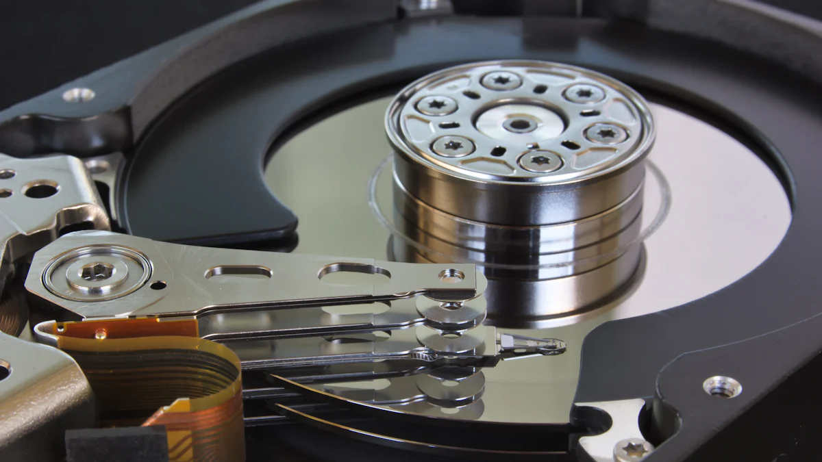
The dual in-line package, or DIP, features a straightforward design with two parallel rows of pins extending from its sides. These pins connect the integrated circuit (IC) inside the package to a printed circuit board (PCB). This layout simplifies soldering and assembly, making it suitable for both manual and automated processes. The symmetrical arrangement of pins ensures easy placement on breadboards and through-hole PCBs. You can also replace components without damaging the surrounding circuitry, which is especially useful during prototyping or repairs.
DIP pin configurations vary depending on the number of pins, which typically range from 8 to 64. The spacing between pins, known as the pitch, is standardized, ensuring compatibility with most PCB designs. This uniformity makes DIP packaging a reliable choice for many applications.
Materials and construction
The construction of a DIP involves several key components. Inside, a silicon die contains the IC, which is connected to the external pins through fine wire bonds. A lead frame supports the structure and provides electrical connections. The package substrate and polymer mold encase the IC, protecting it from physical damage and environmental factors.
DIPs are designed to offer good heat dissipation, which helps maintain the performance and lifespan of electronic components. Compared to surface-mount devices (SMDs), DIPs are larger but easier to handle and install. This makes them ideal for applications where size is less critical but durability and ease of use are priorities.
Common Variants
Ceramic DIPs
Ceramic DIPs (CDIPs) are known for their excellent electrical performance and durability. They are often used in harsh environments where reliability is crucial. The ceramic material provides superior heat dissipation, making these DIPs suitable for high-performance applications. You might find CDIPs in military, aerospace, or industrial systems where components must withstand extreme conditions.
Plastic DIPs
Plastic DIPs (PDIPs) are the most common type of DIP packaging. They are cost-effective and provide good insulation, making them ideal for consumer electronics. The plastic material is lightweight and durable, offering a balance between performance and affordability. PDIPs are widely used in everyday devices, from household appliances to educational kits.
Other types of DIP packages include shrink plastic DIPs (SPDIPs), which have a smaller lead pitch for denser circuit arrangements, and windowed DIPs (CWDIPs), which allow UV light access for erasing EPROMs. Each variant serves specific needs, ensuring that DIPs remain versatile in various applications.
Historical Development of the Dual Inline Package
Early Adoption
Introduction in the 1960s
The dual inline package emerged during the 1960s, a transformative era for the electronics industry. Before its invention, electronic components were housed in bulky packages that made assembly difficult and limited the potential for compact designs. In 1964, Texas Instruments introduced the first DIP, revolutionizing how integrated circuits were mounted. This new design featured a rectangular housing with two parallel rows of pins, simplifying assembly and improving reliability. By the 1970s, the DIP had become the industry standard, playing a pivotal role in advancing technologies like personal computers and consumer electronics.
Role in early integrated circuits
The DIP's introduction marked a turning point for integrated circuits. Its efficient design allowed engineers to create smaller, more reliable devices. Early microprocessors, such as the Intel 8008, utilized this packaging to connect the IC to circuit boards effectively. The DIP's robust construction and compatibility with automated assembly processes made it indispensable for early computing systems. You can trace the success of many early electronic innovations back to the practical advantages offered by this packaging.
Evolution in Electronics
Transition to surface-mount technology
As electronics evolved, the demand for smaller, more efficient components grew. This shift led to the development of surface-mount technology (SMT), which began replacing DIPs in many applications. SMT packages, such as PLCC and SOIC, eliminated the need for through-hole drilling, enabling denser circuit layouts. These components also offered better performance due to shorter lead lengths, which reduced signal interference. Manufacturers embraced SMT for its ability to support automated assembly and cost-effective production. Despite these advancements, DIPs remain relevant for prototyping and educational purposes because of their ease of use.
Continued use in specific applications
Although SMT dominates modern electronics, DIPs still hold value in certain niches. You often find them in legacy systems, where their durability and compatibility with older designs are essential. They also play a role in low-volume production and DIY projects, where their larger size and straightforward design make them easier to handle. While the rise of SMT has reduced the prevalence of DIPs, their simplicity and reliability ensure they continue to serve specific needs in the electronics industry.
Advantages and Disadvantages of DIPs
Key Advantages
Ease of handling and soldering
The dual in-line package stands out for its simplicity and ease of use. Its through-hole mounting design makes soldering straightforward, even for beginners. You can easily align the pins with the holes on a printed circuit board, ensuring a secure connection. This feature benefits both manual assembly and automated processes, making DIP packaging a practical choice for large-scale production.
DIP components also offer mechanical robustness. Their larger size and sturdy construction help them resist stress and vibration, which is especially useful in environments where durability is critical. Additionally, the accessible pin layout simplifies testing and troubleshooting. You can quickly identify and replace faulty components without damaging the surrounding circuit.
Key benefits of DIPs include:
Simplicity in soldering due to through-hole technology.
Mechanical stability against physical stress.
Effective heat dissipation, which enhances component performance.
Compatibility with breadboards and prototyping
DIPs are highly compatible with breadboards and prototyping setups. Their standardized pin spacing of 0.1 inches (2.54 mm) allows for easy insertion into breadboards and sockets. This feature makes them ideal for educational purposes and DIY projects. You can quickly assemble and test circuits without requiring advanced tools or techniques.
The dual inline package also supports both manual and automated assembly processes. This versatility ensures that you can use it in various applications, from small-scale prototyping to larger production runs. Its straightforward design makes it accessible for beginners while remaining reliable for experienced engineers.
Why DIPs excel in prototyping:
Standardized pin configuration ensures compatibility with breadboards.
Easy insertion and removal simplify circuit testing.
Suitable for both manual and automated assembly.
Key Disadvantages
Larger size compared to modern packaging
One of the main disadvantages of dual in-line packaging is its larger size. DIP components occupy more space on a PCB compared to modern surface-mount technology (SMT). This limitation makes them less suitable for applications requiring compact designs.
For example, SMT components can achieve higher density by using smaller packages and closer pin spacing. In contrast, the 0.1-inch pin spacing of DIPs restricts the number of connections you can fit on a circuit board. This difference becomes significant in high-density designs, where every millimeter of space matters.
Aspect | Dual Inline Package (DIP) | Surface-Mount Technology (SMT) |
|---|---|---|
Size | Larger | Smaller |
Pin Spacing | 0.1 inch (2.54 mm) | Variable, often closer spacing |
Suitability for High Density | Less suitable | More suitable |
Limited suitability for high-density designs
DIPs face challenges in high-density or high-frequency applications. Their longer lead lengths can slow down electrical signals, affecting circuit speed. This limitation makes them less effective for sensitive analog circuits or high-frequency designs.
Additionally, the dense pin array can complicate soldering for inexperienced users. While DIPs are easier to handle than SMT components, their larger size and limited pin count restrict their use in advanced applications. These factors highlight the importance of understanding how to choose the appropriate DIP package for your project.
Disadvantage | Description |
|---|---|
Size and Space | DIPs occupy more space on circuit boards compared to modern SMT packaging. |
Limited Pin Count | DIPs generally have fewer pins than newer packaging types. |
Speed Limitations | Longer leads in DIPs can slow down electrical signal travel, affecting circuit speed. |
Soldering Difficulties | The dense pin array can complicate soldering for inexperienced users. |
Not Suitable for High-Frequency Apps | Longer lead lengths can degrade performance in high-frequency or sensitive analog applications. |
By weighing the advantages and disadvantages of dual in-line packaging, you can determine whether it suits your specific needs. While DIPs excel in prototyping and educational settings, they may not be the best choice for high-density or high-frequency designs.
Comparing DIPs to Other Packaging Types
DIPs vs. Surface-Mount Devices (SMDs)
Differences in size and assembly
When comparing the dual in-line package to surface-mount devices, size and assembly methods stand out as key differences. DIPs are larger and bulkier, making them easier to handle during manual assembly. Their through-hole mounting method involves inserting pins into a PCB and soldering them on the back. This process provides greater mechanical stability, which is ideal for applications exposed to physical stress.
In contrast, SMDs are smaller and lighter. They use surface mounting, where components are soldered directly onto the PCB's surface. This method eliminates the need for drilled holes, allowing for more compact circuit designs. However, SMDs are less stable mechanically, which makes them less suitable for environments with significant vibration or stress.
Feature | Dual Inline Package (DIP) | Surface-Mount Device (SMD) |
|---|---|---|
Size | Larger and bulkier | Smaller and lighter |
Assembly Method | Through-hole mounting with soldering on the back | Surface mounting with soldering directly on PCB |
Mechanical Stability | Greater stability, suitable for physical stress | Less stable, but allows for more compact designs |
Cost and application considerations
DIPs and SMDs also differ in cost and applications. DIPs are generally more cost-effective for simple, low-density circuits. Their straightforward design makes them ideal for prototyping and educational purposes. You can easily test and replace components without specialized tools.
SMDs, on the other hand, excel in high-volume production. Their smaller size and compatibility with automated assembly processes reduce overall costs in large-scale manufacturing. This makes SMDs the dominant choice for modern electronics, where compact designs and high efficiency are priorities.
Feature | Dual Inline Packages (DIPs) | Surface-Mount Technology (SMT) |
|---|---|---|
Cost | Lower overall costs in high-volume production | |
Common Applications | Suitable for prototyping and educational purposes | Dominant technology in modern electronics |
DIPs vs. Single Inline Packages (SIPs)
Structural differences
The structural differences between DIPs and SIPs lie in their pin arrangement. A dual in-line package features two parallel rows of pins, which provide a symmetrical layout. This design simplifies placement on breadboards and through-hole PCBs. The even distribution of pins also enhances mechanical stability, making DIPs a reliable choice for robust applications.
SIPs, however, have a single row of pins. This compact structure reduces the space required on a PCB, which is advantageous for designs with limited room. While SIPs save space, their single-row configuration may not offer the same level of stability as DIPs.
Feature | Dual Inline Package (DIP) | Single Inline Package (SIP) |
|---|---|---|
Pin Arrangement | Two parallel rows | Single row |
Stability | Greater mechanical stability | Less stable due to single-row design |
Space Efficiency | Requires more space | More compact |
Use cases for each type
You will find DIPs commonly used in prototyping, educational projects, and applications requiring durability. Their compatibility with breadboards and ease of soldering make them accessible for beginners and hobbyists.
SIPs, on the other hand, are often used in applications where space is a constraint. For example, you might encounter SIPs in power modules or audio amplifiers, where their compact design fits well into tight spaces. While both packaging types serve specific purposes, your choice will depend on the requirements of your circuit design.
Applications of Dual Inline Packages
Educational and Hobbyist Use
Prototyping and DIY projects
DIPs are a staple in prototyping and DIY electronics projects. Their compatibility with breadboards and sockets makes them ideal for testing and development. You can easily insert DIP components into breadboards or prototyping boards without requiring specialized tools. This feature allows you to experiment with circuit designs and make adjustments quickly. DIPs are also included in many educational electronics kits, giving students and hobbyists hands-on experience with real-world components. Their manageable size and straightforward design simplify the process of building and testing circuits.
Common uses of DIPs in prototyping and DIY projects:
Breadboard compatibility for quick circuit assembly.
Easy insertion and removal for iterative testing.
Inclusion in educational kits for practical learning.
Accessibility for beginners
If you're new to electronics, DIPs offer a beginner-friendly introduction. Their through-hole mounting design simplifies soldering, as the extended lead frames align naturally with standard PCB holes. This makes it easier for you to achieve secure connections without much effort. Additionally, the accessible pin layout allows you to connect probes or testing devices directly to the pins. This feature enhances your ability to troubleshoot and refine your designs. Many electronics enthusiasts prefer DIPs for their user-friendly nature, especially when building prototypes.
Why DIPs are beginner-friendly:
Pins simplify testing and troubleshooting.
Ideal for learning and experimenting with circuits.
Industrial Applications
Use in legacy systems
DIPs play a crucial role in maintaining legacy systems. Many older devices, including medical equipment and aerospace electronics, rely on DIP packaging for their integrated circuits. These systems prioritize reliability and stability over miniaturization. If you're working with such systems, DIPs provide a dependable solution. Their robust construction ensures long-term performance, even in demanding environments. You might encounter DIPs in defense systems or industrial machinery where durability is essential.
Role in low-volume production
In low-volume production environments, DIPs shine due to their ease of handling. You can insert and remove them without specialized equipment, making them perfect for prototyping and small-scale manufacturing. Their straightforward design allows for quick assembly and testing, saving time and resources. DIPs are also widely used in educational workshops and electronics classes, where manual handling is common. Their versatility makes them a practical choice for various industrial applications.
Key benefits of DIPs in low-volume production:
Easy insertion and removal.
Suitable for prototyping and testing.
Reliable performance in critical systems.
Automotive and Specialized Fields
Applications in older automotive electronics
In older automotive electronics, DIPs are indispensable. They are commonly used in systems like engine control units and entertainment systems. These components ensure reliability and stability, which are vital for vehicle performance and safety. If you're working on automotive designs, DIPs offer durability and dependability. Their straightforward design makes them easier to handle and solder manually, which is especially useful in repair and maintenance tasks.
Use in niche designs
DIPs continue to find use in niche electronic designs. Their dual in-line arrangement facilitates easy soldering and assembly, whether you're working manually or using automated processes. They also provide excellent heat dissipation, which helps maintain performance and extend the lifespan of components. In specialized fields like defense and aerospace, DIPs are valued for their ruggedness and reliability. These sectors prioritize durability over miniaturization, making DIPs a preferred choice for critical systems.
Advantages of DIPs in niche designs:
Easy soldering and assembly.
Good heat dissipation for reliable performance.
Rugged construction for demanding applications.
The Future of Dual Inline Packages
Continued Relevance
Importance in prototyping and education
The dual in-line package continues to play a vital role in prototyping and education. Its straightforward design makes it an excellent choice for hands-on learning. You can easily insert DIPs into breadboards or solder them onto perfboards, which simplifies circuit assembly. This accessibility allows you to focus on understanding the fundamentals of electronics without worrying about complex tools or techniques.
DIPs also excel in prototyping because of their ease of handling. You can quickly insert and remove components during testing, enabling rapid modifications to your design. Their bulkier size, while a drawback in some applications, becomes an advantage here. It provides a manageable platform for experimenting with circuits, especially for beginners. Whether you're a student or a hobbyist, DIPs offer a reliable and user-friendly way to explore electronics.
Why DIPs remain relevant in prototyping and education:
Easy insertion into breadboards.
Simple soldering process for perfboards.
Ideal for frequent component adjustments.
Manageable size for hands-on learning.
Niche Applications
Support for legacy systems
DIPs remain indispensable in maintaining legacy systems. Many older devices, including industrial machinery and medical equipment, rely on DIP packaging for their integrated circuits. These systems often prioritize reliability over miniaturization, making DIPs a perfect fit. If you're working with legacy systems, you’ll appreciate the durability and stability that DIPs provide. Their robust construction ensures long-term performance, even in demanding environments.
In addition, DIPs offer compatibility with older PCB designs, which simplifies repairs and replacements. This makes them a practical choice for industries like aerospace and defense, where maintaining existing systems is critical. By supporting legacy systems, DIPs continue to serve as a bridge between past and present technologies.
Challenges and Opportunities
Competition with modern packaging
DIPs face significant challenges when competing with modern packaging technologies. Surface-mount devices (SMDs) dominate the market due to their smaller size and higher efficiency. In comparison, DIPs occupy more space on a PCB, which limits their use in miniaturized electronics. Their limited pin count and longer lead lengths also restrict their functionality in high-density and high-frequency applications.
Challenge | Description |
|---|---|
Size and Space | DIPs take up more room on circuit boards compared to modern SMT packages. |
Limited Pin Count | Fewer pins reduce their versatility in complex designs. |
Speed Limitations | Longer leads slow down electrical signals, affecting circuit performance. |
Not Suitable for High-Frequency | Lead length and inductance issues make them less effective in high-frequency applications. |
Despite these challenges, DIPs retain their relevance in specific niches, such as prototyping and legacy systems. Understanding these limitations helps you decide when DIP packaging is the right choice for your project.
Potential for innovation
The future of DIP packaging holds exciting opportunities for innovation. Advances in materials science could lead to the development of new substrates that improve thermal conductivity, mechanical strength, and electrical properties. These improvements would make DIPs more suitable for high-power and high-frequency applications.
Emerging technologies like additive manufacturing also open new doors. For example, 3D printing allows for customized DIP designs tailored to specific needs. This capability enables rapid prototyping and faster time-to-market for new products. Additionally, the rise of IoT and smart technologies creates opportunities for DIPs in applications like sensors and smart infrastructure. By embracing these innovations, DIPs can evolve to meet the demands of modern electronics while retaining their core strengths.
Opportunities for DIP innovation:
Enhanced materials for better performance.
Customization through 3D printing.
New applications in IoT and smart technologies.
The future of DIPs lies in balancing their traditional strengths with modern advancements. By adapting to new challenges and leveraging emerging technologies, DIPs can continue to serve as a valuable component in electronics.
The dual inline package has played a transformative role in PCB design and manufacturing. Its straightforward design simplifies assembly, making it ideal for prototyping, education, and legacy systems. You benefit from its durability, ease of soldering, and accessibility during testing. However, its larger size and limited pin count make it less suitable for compact, high-density designs.
DIPs remain relevant in prototyping and educational settings, where their simplicity supports hands-on learning. Innovations like shrink DIPs show their adaptability to modern demands. As electronics evolve, DIPs continue to bridge traditional and modern practices, ensuring their place in specific applications.
FAQ
What is the main purpose of a dual inline package (DIP)?
A DIP simplifies circuit assembly by providing a straightforward pin layout. You can use it for prototyping, educational projects, and legacy systems. Its design ensures durability and ease of handling, making it ideal for beginners and professionals alike.
How do DIPs differ from surface-mount devices (SMDs)?
DIPs use through-hole mounting, while SMDs attach directly to the PCB surface. DIPs are larger and easier to handle. SMDs save space and suit high-density designs. You’ll find DIPs better for prototyping, while SMDs dominate modern electronics.
Why are DIPs popular in educational settings?
DIPs are beginner-friendly. Their standardized pin spacing fits breadboards, making circuit assembly simple. You can easily solder or replace components without advanced tools. This accessibility helps students and hobbyists learn electronics through hands-on experimentation.
Can DIPs handle high-frequency applications?
DIPs are less effective for high-frequency designs. Their longer lead lengths can slow electrical signals and cause interference. For high-speed circuits, you should consider surface-mount technology or other advanced packaging options.
Are DIPs still used in modern electronics?
Yes, DIPs remain relevant in specific niches. You’ll find them in prototyping, legacy systems, and low-volume production. Their simplicity and durability make them valuable for applications where size and density are less critical.
What materials are used to make DIPs?
DIPs are typically made from plastic or ceramic. Plastic DIPs are lightweight and cost-effective, while ceramic DIPs offer better heat dissipation and durability. You can choose the material based on your application’s requirements.
How do you solder a DIP onto a PCB?
Insert the DIP’s pins into the PCB holes. Apply solder to each pin on the opposite side of the board. Ensure the solder flows smoothly for a secure connection. You can use a soldering iron and basic tools for this process.
What are the limitations of DIPs?
DIPs take up more space on a PCB and have fewer pins compared to modern packaging. They’re unsuitable for compact, high-density designs. Their longer leads can also affect performance in high-frequency circuits. You should evaluate these factors before choosing DIPs.
See Also
Exploring The Development Of Single Inline Packages Over Time
Essential Circuit Board Components For New Electronics Enthusiasts
A Guide To Calculating Poles In Amplifier Design
Key Functions Of Circuit Board Components In Electronics
How To Calculate And Understand Potentiometer Loading Errors